


 Development Kit
 Mouse over to zoom in
- Product 2/6
-


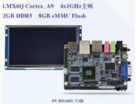
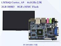
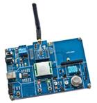
Cortex-M4 M0 dual core processor: LPC4357 core board, downward compatibility LPC4350, LPC4330, LPC4320, LPC4310, LPC4353, LPC4337, LPC4333, Pin to Pin LPC1850, LPC1857
Core board size: 57.2 * 77.2 mm
Base board size: 141*168 mm
Expansion board size: 165*112.8 mm
Example Program Characteristics
1 Operating system:
RTX - V4.60; Keil operating system
FreeRTOS - V7.3.0
μC/OS-III - source
2 File system:
RL-FlashFS - V4.22; Keil file system, support FAT12, FAT16 and FAT32 file system, the file system can be used in the SD card, Nand Flash, U disk, provide bad block management function of Nand Flash. FatFs - R0.09a; source
3 Network protocol stack:
RL-TCPnet - V4.60; Keil's own network protocol stack.
Lwip - V1.4.0
4 Graphics library:
EmWin - V5.16; a new version of C/GUI
EmWin - V5.18; a new version of C/GUI,
SWIM -- graphics library, source code.
5 USB:
RL-USB - V4.60; Keil comes with the USB protocol stack, support ADC, CDC, HID, MSC class from the equipment, the main controller supporting HID and MSC.
LPC-USB - provides the USB protocol stack, with source code, from the equipment already provides a mouse, keyboard, audio, CDC, large capacity equipment drive program, the main control provides keyboard, audio, large capacity equipment driver source code
Processor Parameters
1 Cortex-M4 Processor
- running at frequencies of up to 204 MHz
- Memory Protection Unit (MPU)
- Nested Vectored Interrupt Controller (NVIC)
- Hardware floating-point unit
- Non-maskable Interrupt (NMI) inpu
- JTAG and Serial Wire Debug (SWD), serial trace
- ETM and ETB support
- System tick timer
- Four reduced power modes: Sleep, Deep-sleep, Power-down, Deep power-down
2 Cortex-M0 Processor core
- capable of off-loading the main ARM Cortex-M4
- running at frequencies of up to 204 MHz
- JTAG, Serial Wire Debug, and built-in NVIC
3 On-chip memory
- Up to 1024kB dual bank Flash
- 136 kB SRAM for code and data use
- 16 kB on-chip EEPROM data memory.
- 64 kB ROM containing boot code, on-chip SW drivers
- 128 bit One-Time Programmable (OTP) memory
4 Clock generation unit
- Crystal oscillator (operating range of 1 MHz to 25 MHz)
- 12 MHz internal RC osc.
- Ultra-low power RTC crystal osc.
- On-chip PLL allows CPU operation up to the maximum CPU rate
5 Serial interfaces
- Quad SPI Flash IF (SPIFI)
- 10/100T Ethernet MAC (RMII and MII IF)
- HS USB 2.0 Host/Device/OTG IF
- HS USB 2.0 Host/Device IF
- 4 550 UARTs
- 2 C_CAN 2.0B controller with one channel
- 2 SSP controllers
- SPI controller
- Fast-mode Plus I2C-bus IF
- standard I2C-bus IF
- 2 I2S IFs
6 Digital peripherals
- External Memory Controller (EMC)
- LCD controller
- SD/MMC card IF
- 8-channel General-Purpose DMA (GPDMA) controller
- Up to 164 General-Purpose Input/Output (GPIO) pins
- 4 general-purpose timer/counters
- motor control PWM for three-phase motor control
- Quadrature Encoder IF (QEI)
- Repetitive Interrupt timer (RI timer)
- Windowed watchdog timer
- Ultra-low power Real-Time Clock (RTC)
- Alarm timer
7 Analog peripherals
- 10-bit DAC
- 2 10-bit ADCs
8 Security
- AES engine programmable through an on-chip API
- 2 128-bit secure OTP memories (AES key storage, customer use)
- Unique device ID
Onboard Information
1) 128MBit SDRAM (32Bit)
2) 128MBit NOR Flash (2 form 32Bit)
3) 32 Mbit SPI Flash
4) 256Kbit IIC EEPROM
5) SD memory card interface (SDIO mode)
6) 10 pin 2.0mmJTAG interface
7) 10/100M Ethernet interface
8) USB2.0 (full speed built-in PHY) slave device interface
9) USB2.0 (full speed built-in PHY master device interface)
10) USB2.0 (high speed built-in PHY) slave the device interface
11) USB2.0 (high speed built-in PHY) master device interface
12) 2 road RS232 interfaces
13) 2 road CAN interfaces
14) microphone input interface
15) Dual channel audio input interface
16) Dual channel audio output interface
17) Dual channel Headset interface
18) Mono speaker interface
19) 1 five way navigation button
20) 3 function keys
21) 5controlled LEDs
22) A button battery holder (without battery)
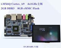
23) 24bit LCD interface (the standard 4.3 inch LCD with touch screen)
24) Data bus EMC_D0 core board -- EMC_D31 and EMC_A0 -- EMC_A23 extraction
25) Most of the JTAG core board in addition to occupy the I/O extraction
Shipping List
1* LPC4357 development board
1* 7 Inch Touch Screen
1* crossover cable
1* Serial port extension of line
1* High speed Mini USB line
1* 5V power adapter
Development tools
ULINK2
Does not recommend the use of JLINK (JLINK protection measures is not enough, the electrostatic computer come easy to burn out JTAG)
-
- $228.00
-
- $234.00
-
- $202.00
-
- $1.99
-
- $12.90
-
- $55.00